
IPKISS Design Environment
The IPKISS design environment is a complete platform for Integrated Photonics Design. Through EUROPRACTICE the following modules are available:
- IPKISS Photonics Design Platform
- Link for Siemens EDA (Formerly IPKISS.eda functionality)
- Link for Ansys Lumerical
- Link for CST
IPKISS Photonics Design Platform
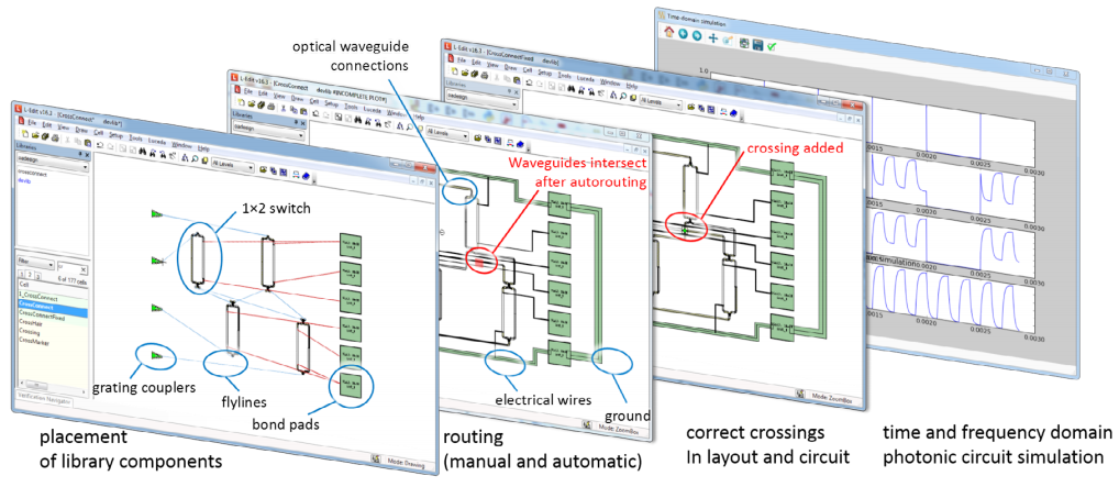
IPKISS is a Python scripting environment that covers the complete photonic IC design flow up to measurement feedback for true component validation. The components rely on a single, centrally defined model for a smooth transition between the different design stages such as layout component simulation and circuit simulation. IPKISS raises the integrity of your design flow, via:
- Fully parametric powerful Python scripting
- From netlist to layout in the same component
- Circuit simulation & validation
- Customizable to internal design methodology
Key Features:
Python User Interface- Python parametric design framework
- Python: easy, industry standard scripting language
- Define building blocks in one place: reduce copy/paste and translation between tools
- Extract and exchange information between different representations ("views") from a single definition: layout, 3D model, circuit connectivity
- Hierarchical component management
- Photonic waveguide definitions: flexible cross sections, parametric bend algorithms
- Semi-automatic routing
- GDSII import/export
- Predefined waveguide definitions: strip, rib, slot, multi-level
- Splitters, couplers, bends, crossings, apertures
- Fiber couplers: line grating coupler, curved grating coupler, inverted taper
- Filters: MMI, Mach-Zehnder interferometer, (multi-)ring resonator, in-line gratings
- Photonic crystals: 1D and 2D photonic crystals including photonic crystal cavities
- I/O: components
- Containers: Extend, fanout, reroute, terminate, auto transitioning ports
- Alignment markers, fiducials
- Virtual fabrication: generate 2D and 3D Models for rendering and Physical simulation
- Interface with third-party tools
- IPKISS-Siemens EDA Interoperability
- IPKISS-Ansys Lumerical Interoperability
- IPKISS-CST Interoperability
- CAMFR: Mode solver
- Optimization, post-processing, visualizations
- S-matrix extraction
- Compact model building
- CAPHE: Optical Network Solver
- Layout aware: correct waveguide lengths by design
- Frequency and time-domain simulation
- Equation based source definition
- Compact/Behavioral-model based circuit simulation from the Python script UI
- Optimization
- Tolerance analysis
Link for Siemens EDA
The Link for Siemens EDA plugs into the Luceda Photonics Design Platform and enables you to export parametric cells to the GUI of L-Edit and L-Edit Photonics by Siemens EDA.
Specialized photonic components require a scripted approach with version and quality control to handle the complexity and the need for customization. These specialized components are designed within a component library built on top of a PDK technology.
IPKISS is well-suited for the design of specialized components and library IP management. It provides the quality backbone of IP generation. Export your IPKISS libraries to OpenAccess and deploy them in L-Edit Photonics, where you finalize your designs through optical and electrical routing, final design assembly, mask preparation and design verification.
PIC designer benefits:
- Complement the power of Luceda IPKISS with the features of L-Edit and L-Edit Photonics.
- Create and manage your parametric design libraries with IPKISS' code-based approach.
- Enhance your team collaboration with shared common libraries and version control.
- Drag and drop IPKISS parametric cells and deploy your IP libraries inside L-Edit.
- OpenAccess database automation and PDK management (OaScript).
- Benefit from a validated design flow that provides access to more than 20 foundry PDKs.
Link for Ansys Lumerical
Link for CST
Define your layouts and simulation recipes using the Luceda IPKISS Photonics Design Platform.
- Use "Link for Ansys Lumerical" to run in Lumerical FDTD or MODE EME.
- Use "Link for CST" to run in 3DS Simulia CST Studio Suite (FDTD).
PIC designer benefits:
- Manage the complete design flow from one single place, including physical simulations with a third-party tool.
- Minimize design errors by controlling your layouts directly at the source.
- Leverage the IPKISS 3D virtual fabrication to create a 3D model of your designs based on the correct FAB process and technology information.
- Integrate the simulation results into IPKISS circuit models and link them to your layouts automatically.
- Take advantage of the IPKISS Python-based design flow to optimize your designs and generate parameter sweeps.
Available PDK's:
-
Silicon (Production)
- AIMphotonics
- AMFSiP
- CompoundTek
- IHP SG25H5
- imec iSiPP50G
- imec iSiPP200
- IMECAS
- Leti Si310 W300
- OpenLight
- SITRI
- TowerSemi PH18 Silicon (Prototyping)
- Australian Silicon Photonics
- CORNERSTONE SOI
- SiEPIC
- SiEPIC Shuksan
- SiPhotonIC Silicon Nitride
- CORNERSTONE SiN
- imec BioPIX
- Ligentec AN800
- Ligentec AN150
- LioniX TripleX 1550
- LioniX TripleX Visible Indium Phosphide
- Fraunhofer HHI
- SMART Photonics
- SMART Photonics Gen 2 Packaging
- Tyndall