
Free Trial
IntelliSense are offering EUROPRACTICE members a free 30-day
evaluation license of their products. This will allow new users to
evaluate any IntelliSense product and existing users to evaluate
additional products. If you wish to take advantage of this offer,
please contact the Microelectronics Support Centre at RAL.
MicroelectronicsCentre@stfc.ac.uk
Evaluation Licenses
IntelliSense make available a wide range of closely integrated tools for the MEMS and Microsystems designer to seamlessly go from schematic capture and optimization to design verification and tapeout. A flexible design flow allows you to start your design at either schematic, layout or 3D level.
IntelliSuite Comprehensive
IntelliSuite Comprehensive is a tightly integrated design
environment. IntelliSuite allows the design, process, packaging
and system teams collaborate on MEMS devices that can be
prototyped and manufactured with fewer costly iterations.
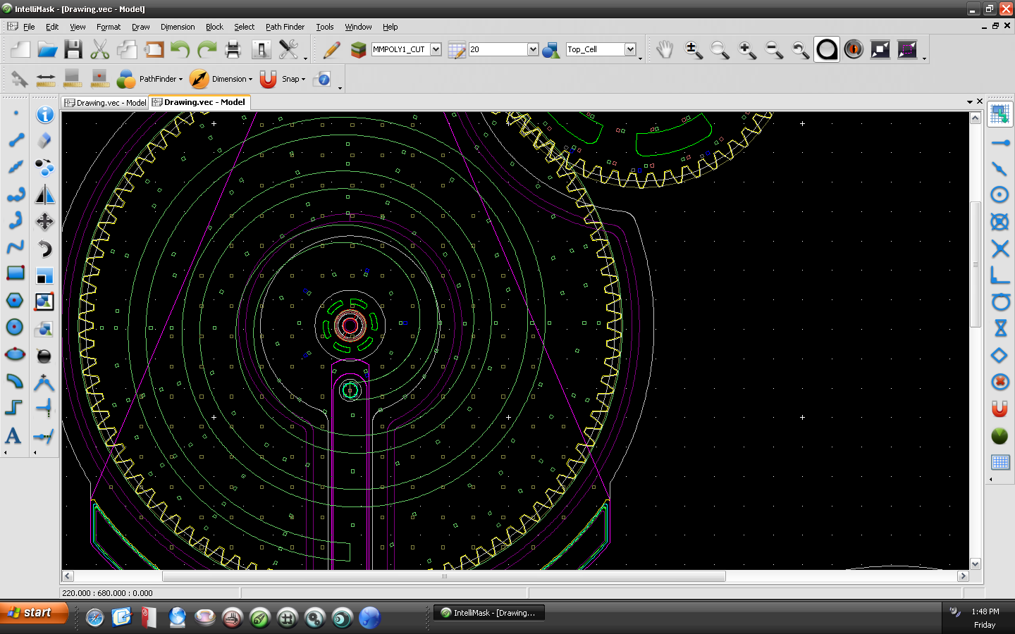
Blueprint is a layout tool specifically designed for the
MEMS community. Blueprint includes TapeOut, an all-angle Physical
Verification (DRC) tool, and a language-independent scripting
tool, enabling you to create complex designs through scripting.
The built-in Cross-Section Viewer allows you to view mask
cross-sections and export them to PowerPoint. Automated hexahedral
meshing techniques can be used to construct robust meshes for
analysis.
RECIPE is a powerful, easy-to-use RIE/ICP (Reactive Ion Etch/Inductive Coupled Plasma) etch process simulation tool for use in designing microstructures. With RECIPE, you can layout your microstructure and automatically simulate isotropic, RIE, ICP/Bosch/DRIE etching or any combination of the three processes. RECIPE supports the simulation of both ion-assisted etching and deposition processes.
IntelliSuite Plus
IntelliSuite Plus contains all the modules and features of
IntelliSuite Comprehensive plus the following additional products.
Exposure is a lithography simulator that analyses the
physical phenomenon and chemical reaction of SU-8 photoresists
during the exposure, PEB (Post Exposure Bake), and development
process which are the focuses of UV lithography modeling. Exposure
can predict the developed profiles of SU-8 photoresists. Also, it
can analyse the intensity distribution impact on the developed
profile of SU-8 photoresists.
The FabSim process simulator enables users to quickly
create photo-realistic process models and cross-sections using
full physical simulation, rather than traditional geometrical
methods. FabSim is a visualizer that enables you to view and debug
your complex process flow. FabSim works with IntelliFab to render
each process step in vivid detail. Users can view their structure
at each process step and view cross sections at any angle for
easier debugging.
IntelliEtch allows one can pattern and etch any surface
orientation, expanding the possibilities of MEMS design and
enabling the testing of vicinal surface effects. Furthermore,
IntelliEtch makes possible the patterning and etching of non-flat
substrates with flat, round, vertical, or diagonal features. Even
spherical silicon samples can be patterned and etched. It is also
possible to explore and fine-tune a particular process by etching
a structure atom-by-atom.
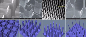
NanoViewer allows the designer to make a simple and
efficient comparison among different silicon samples. With just a
basic SEM image, users can easily generate a 3D reconstruction,
take snapshots, and even export 3D models in a variety of popular
CAD formats. In addition, users are able to quickly perform
measurements and acquire useful information about the sample's
surface, like its roughness.
BioMEMS and Microfluidics Option
BioMEMS and Microfluidics analysis datasheet
The BioMEMS and Microfluidics Option provides additional
functionality to either the IntelliSuite Comprehensive or the
IntelliSuite Plus products.
The Microfluidics analysis module is a full 3D Navier-Stokes solver
optimised for microfluidic applications. Support has been included
for electrokinetic phenomena, Red-Ox reactions, acids, bases,
ampholytes and fluid structure interaction.
Advanced visualisation algorithms allow the designer to look at
cross-sectional profiles, velocity vectors and transient results.
Using the Microfluidics analysis module the designer can
investigate:
- Fluid flow and fluid dynamics
- Electrodynamics (time varying or constant electric fields)
- Electrokinetics
- Stochiometry and reaction kinetics (acids, bases, ampholytes, multi-valent analytes)
- Mass transport
- Heat transfer
- Electrochemistry
- Fluid structure interaction
- Particulates such as DNA, microspheres for dielectrophoresis and separations
The technical brochure below, in Adobe Acrobat format, provides further information on the IntelliSense BioMEMS and Microfluidics analysis system.
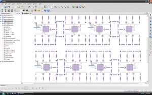
SYNPLE
SYNPLE datasheet
SYNPLE allows you to capture your MEMS at a schematic level. Your
design can then be quickly iterated and optimized at different
granularities. Sophisticated synthesis algorithms can
automatically convert your schematic into mask layout, 3D or
better yet a meshed structure for full multiphysics analysis.
SYNPLE includes state-of-the-art schematic capture and simulation
tools allowing you to take a hierarchical approach to the design
space. SYNPLE provides a large multi-domain library of electrical,
mechanical, thermal, and MEMS libraries. These elements may be
combined in an effortless drag-and-drop fashion and then wired to
create schematics of multi-domain systems. As a result, you can
quickly survey a large design space before initiating a detailed
analysis and verification process.
Users can perform device-level optimization using Design of
Experiments (DoE), Robust Design or other techniques. Built-in
place-and-route and synthesis algorithms can be then used to
convert the schematic into a mask layout or an optimally
hexahedral meshed model ready for full 3D analysis.
More Information
Operating Systems
IntelliSuite
- Windows 7 Professional 64-bit
SYNPLE
- Windows 7 Professional 64-bit